Facilities, Equipment, and Other Resources
Temple University
Physics and ICMS (Michael Klein, John Perdew, Adrienn Ruszinszky)
+ Facilities
| Facility | Description (capacity, capability, etc.) | Relative Proximity | Availability to Project | Relevance to project |
|---|---|---|---|---|
| Nano Instrumentation Center | Electron microscopy, Energy dispersive spectrometer, e-beam lithography | College of Engineering, Temple University | Available for subscription fee | High, sample characterization and device preparation |
| Library and Web of Science | Physical and electronic access to journal articles and books | Temple | Yes | Source of scientific information |
| CVD Lab | This lab of 860 ft2 in area is equipped with several HPCVD systems for MgB2 thin films, multilayers, and coatings. One HPCVD system consists of two stainless steel tube reactors, one for 1 cm x 1 cm films and one for 2 dia. films. An integrated HPCVD system consists of two HPCVD reactors, one sputter system, and a central distribution system that transfers thin films between the chambers under vacuum, allowing deposition of MgB2 multilayers in situ. | Prof. Xis lab at Temple University. | Available to the project. | The proposed CVD system for single-layer and few-layer MoS2 films will be in this lab. |
| Clean Room | This facility has a class-100 area of 220 ft2 and a class-1000 area of 220 ft2. It is equipped with a Suss Microtech MJB4 mask aligner, a Kurt J. Lesker sputtering system, a reactive ion etcher, an IntlVac Nanoquest I ion beam etching system, and other photolithography equipment such as spinner, microscope, furnace, etc. | In the Physics Department at Temple University. | Available to the project. | For patterning of the few-layer MoS2 films for electrical measurement. |
| Electrical Characterization Lab | This lab includes a shielded area of 260 ft2 for low noise device measurement, and a general measurement area of 260 ft2. Various electrical characterization instruments are available for R vs T, I vs V, C vs T, C vs V, tan? vs T, and tan? vs V measurements, tunneling characterization such as I - V, dI/dV , Ic - B, and Shapiro step measurements, ferroelectric testing, measurements in magnetic field up to 7 T in the temperature range from 1.5 325 K, and microwave measurement with a microwave network analyzer and a dielectric resonator. | Prof. Xis lab at Temple University. | Available to the project. | Electrical measurement of the single-layer and few-layer MoS2 films will be in this lab. |
| Materials Research Facility | The facility has a thin film x-ray diffraction system (Bruker D8 DISCOVER Diffractometer System), a transmission electron microscope (JOEL JEM-1400 TEM), and an atomic force microscope (Veeco DIMENSION ICON System). | In College of Science and Technology at Temple University. | Available to the project. | Structural characterization of the single-layer and few-layer MoS2 films. |
| Penn Regional Nanotechnology Facility (PRN) | The facility has several SEM and TEM systems, and an FEI Strata DB235 Focused Ion Beam system. | University of Pennsylvania, 4 miles from Temple University | Available to the project with user fees. | Structural characterization of the single-layer and few-layer MoS2 films. |
| Centralized Research Facilities | The facility has several Raman and FTIR spectrometers, several SEM and TEM systems, an FEI Strata DB235 Dual Beam SEM-Focused Ion Beam system, and various microfabrication tools such as Karl Zuss MJB-3 Mask Aligner and a Deep Reactive Ion Etching system. | College of Engineering, Drexel University, 4 miles from Temple University | Available to the project with user fees. | Structural characterization of the single-layer and few-layer MoS2 films. |
| Rutgers Institute for Advanced Materials, Devices and Nanotechnology | The facility provides Rutherford backscattering Spectroscopy service. | Rutgers University in Piscataway, NJ. | Available to the project with user fees. | Structural characterization of the single-layer and few-layer MoS2 films. |
| Owl's Nest Linux cluster for high-performance computing. | ~2000 computational cores. Part of the cluster (9 nodes) is dedicated to GPU computing using Nvidia Tesla and AMD FirePro3d GPUs. |
The cluster is hosted and operated by Computer Services and the College of Science of Technology at Temple University. | Access to the cluster is constantly available to members of the Temple community. | The cluster, which consists of multiple sub-sections each with a different hardware configuration, is a flexible resource allowing both memory intensive and moderate-size parallel computational tasks; it is suitable for both first- principles and coarse-grained MD simulations. |
| Owls Nest 2 Linux cluster for high-performance computing. | Funded by NSF, currently under construction, and planned to be online within the next 6 months. 6448 computational cores. 176 x 14-core nodes for conventional |
The cluster will be hosted and operated by Computer Services and the College of Science of Technology at Temple University. | Access to the cluster is constantly available to members of the Temple community. | The cluster, which will consist of multiple sub-sections each with a different hardware configuration, will be a flexible resource allowing both memory intensive and moderate-size parallel computational tasks; it is suitable for both first-principles and coarse-grained MD simulations. |
| High Performance Computer Cluster (EFRC) | 1440 computational cores (72 nodes, 20 cores/node), 128 GB RAM per node, 2-level infiniband FDR fabric
for message passing and storage access. 2 100 TB Storage servers |
Temple University | Available to EFRC members at Temple University. Can be made available to outside collaborators. | Suitable for first-principles calculations and large-scale molecular simulations. |
| Compute.temple.edu shared workstation | 64 computational cores (4 x 16-core AMD Opteron 6380), 512 GB RAM, 120 TB storage | Temple | Available to EFRC members at Temple University. Can be made available to outside collaborators. | Suitable for memory intensive and parallel computations. |
| 2 EFRC shared AMD workstations | Each have 32 computational cores ( 4 x 8-core AMD Opteron 6328 3.2 GHz) and 512 GB RAM | Temple | Available to EFRC members at Temple University. Can be made available to outside collaborators. | Suitable for memory intensive and parallel computations. |
| 3 EFRC shared Intel workstations | Each have 28 computational cores ( 2 x 14-core Intel Xeon E5-2690v4 2.60 GHz) and 768 GB RAM | Temple | Available to EFRC members at Temple University. Can be made available to outside collaborators. | Suitable for high-memory, parallel computations. |
| NIH Cluster | 1360 computational cores (60 with 10-cores & 128 GB RAM each + 10 nodes for GPU computation)
10 nodes reserved for GPU-based computations, each with 4 x Nvidia Geforce TITAN X, 2 x 8-core Intel Xeon E5-2640v3 2.60 GHZ, and 12 GB RAM |
Temple | Available to Klein group | Suitable for large scale molecular simulations |
| NERSC computer cluster in Lawrence Berkeley National lab | Award in 2014 ~ 2.5 Million computer hours with access of thousands of cores in parallel computational jobs | Remote computer assess | Available, renewable every year | Related |
| XESDE computer cluster award | Award in the period 2013-2014 about 1.8 M computer hours | Remote computer assess | Available, renewable every year | Related |
+ Equipment
| Equipment | Description (capacity, capability, etc.) | Location | Relevance to project |
|---|---|---|---|
| 300 mK UHV STM | 300 mK- UHV in magnetic field up to 9 Tesla STM with option of UHV surface preparation | Temple University (Dr. Iavarones lab) | High- STM characterization of single crystals, thin films and few layers and heterostructures of dichalcogenides |
| 4 K STM | 4.2 K STM in magnetic field up to 9 Tesla | Temple University (Dr. Iavarones lab) | High- STM characterization of single crystals, thin films and few layers and heterostructures of dichalcogenides |
| LEED/Auger | Energy Electron Diffractrometer with an Auger spectrometer (OCI BDL800IR), | Temple University (Dr. Iavarones lab) | High |
| Triple source e-beam evaporator | triple cell e-beam source evaporator (Omicron) | Temple University (Dr. Iavarones lab) | High- will be used to deposit atoms on the surface of single crystals, films and few layers of dichalcogenides. |
| Bonder | West Bond bonder | Temple University (Dr. Iavarones lab) | Modest, to make contacts for small samples and devices |
| Integrated HPCVD system | This system consists of two HPCVD reactors, one sputter system, and a central distribution system. | In Prof. Xis lab, Temple University. | One of the chambers will be modified into a CVD system for the single-layer and few-layer MoS2 films. |
| UHV sputter system | The Kurt J. Lesker UHV sputtering system is used for various metallization layers. | In the clean room, Physics Department, Temple University. | For depositing metal contacts for electrical measurements. |
| Bruker AXS D8 Discover Thin Film X-Ray Diffractometer | The Bruker AXS D8 Discover system is a powerful tool for analyzing the structure of thin film samples, including the phase, lattice parameters, and strain. In particular, using grazing incidence, the x-ray scatters on lattice planes perpendicular to the sample surface, allowing the direct determination of the in-plane lattice constant, lattice mismatch and crystal symmetry, ideal for studying strain and strain relaxation in very thin epitaxial layers. | In the Materials Research Facility, College of Science and Technology, Temple University. | Characterization of phase, lattice parameters, and strain in the single-layer and few-layer MoS2 films. |
| Veeco Dimension Icon-PT Scanning Probe Microscope | The Veeco Dimension Icon system can perform Atomic Force Microscopy, Piezo Force Microscopy, Electric Field Microscopy, and Magnetic Force Microscopy. | In the Materials Research Facility, College of Science and Technology, Temple University. | Characterization the number of layers in the single-layer and few-layer MoS2 films. |
| PPMS System | The QuantumDesign Physical Property Measurement System allows measurement of transport properties in magnetic fields up to 9 T and at temperatures from 1.8 to 400 K. | Prof. Chens lab in the Physics Department at Temple University. | Transport measurement of the single-layer and few-layer MoS2 films. |
| Raman scattering system | The Raman scattering system has a SPEX Triplemate spectrometer equipped with a liquid-nitrogen-cooled multichannel coupled-charge-device detector. | In Prof. Xis lab, Temple University. | Characterization the number of layers in the single-layer and few-layer MoS2 films. |
+ Other Resources
| Other Resources | Description (capacity, capability, etc.) | Relative Proximity | Availability to Project | Relevance to project |
|---|---|---|---|---|
| Machine shop | Custom needs | Temple University-College of Science and Technology | Available to PI | Modest |
| Electronic shop | Custom Needs | Temple University-College of Science and Technology | Available to Pi | Modest |
| VASP | PAW electronic structure of solids and supercells | License and source code at Temple | Yes | For most of the materials computations. |
| Materials Studio | Geometry and visualization of solids and supercells | License and code at Temple (Ruzsinszky) | Yes | For most of the materials computations |
| BAND and ADF | All-electron electronic structure of solids and molecules | License and source code at Temple | Yes | For some materials computations |
| GAUSSIAN-03 | All-electron electronic structure of molecules and solids | License and source code at Temple | Yes | For some materials computation |
Chemistry (Eric Borguet, Daniel Strongin, Michael Zdilla)
+ Facilities
| Facility | Description (capacity, capability, etc.) | Relative Proximity | Availability to Project | Relevance to project |
|---|---|---|---|---|
| Renovated Laser Laboratory | (~100 m2) providing temperature, humidity and dust control for state-of-the-art laser facility. | In PI building | Available | |
| Renovated microscopy laboratory | (~30 m2) providing temperature, humidity and dust control for state-of-the-art microscopy (AFM, STM,) | In Building | Available | |
| Renovated wet chemistry and materials preparation/characterization laboratories | (~ 40 m2 total) with Nanopure water purification units. | In Building | Available | |
| Experimental Laboratory | 100 sq. feet synthesis lab with 6 fume hoods | In Building | Fully available | Synthesis, kinetic measurements. |
| Center for Functional Nanomaterials | Electron Microscopy facility | BNL | Through collaboration with Co-PI (Zhu) | Detailed analysis of the geometric and electronic structure of the designed materials |
| NSLS | XAS, photoelectron spectroscopy | BNL | General user proposal | XAS characterization of photocatalytic materials. |
+ Equipment
| Equipment | Description (capacity, capability, etc.) | Location | Relevance to project |
|---|---|---|---|
| B Nanosecond Nd.YLF. 527 nm (and 1054 nm), 10 mJ, single shot - 5 kHz | Beury | ||
| Picosecond/Femtosecond Ti:Sapphire Regenerative Amplifier (BMI/Coherent) 1 kHz, 800 nm, 0.8 mJ to pump Infrared Optical Parametric Amplifier (OPA) 25 fs-4 ps, 1.1 - 4 ľm, > 10 ľJ | for Linear & Nonlinear (SHG, SFG) Optical Spectroscopy & Dynamics experiments | Beury | |
| Ultrashort (<25 fs) Ti:Sapphire Oscillator, tunable 725-930 nm (< 100 fs) & harmonics | for Linear & Nonlinear (SHG, SFG) Optical Spectroscopy & Dynamics experiments | Beury | |
| Femtosecond Ti:Sapphire Regenerative Amplifier (Quantronix) 1 kHz, 800 nm, 3.5 mJ to pump Infrared Optical Parametric Amplifier (OPA) 1.1 -5 ľm > 30 ľJ, 5 -15 ľm > 15ľJ | for Linear and Nonlinear (SHG, SFG) Optical Spectroscopy and Dynamics experiments | Beury | |
| Femtosecond Ti:Sapphire Regenerative Amplifier (Coherent-LIBRA) 1 kHz, 800 nm, 5 mJ used to pump Infrared Optical Parametric Amplifier (TOPAS-OPA), 1.1 -2.6 ľm, > 1.5 mJ total output | for Linear & Nonlinear (SHG, SFG) Optical Spectroscopy & Dynamics experiments and development of ultrabroadband OPAs | Beury | |
| Optics, photon detection equipment (APD, CCD, IR detectors), spectrographs, data acquisition and analysis | Beury | ||
| Two Scanning Tunneling/Atomic Force Microscopes (Molecular Imaging, Agilent) especially adapted | for imaging in ambient and under liquid/electrochemical environment and current sensing AFM | Beury | |
| Electrochemical Potentiostats, Bipotentiostat and Galvanostat | Beury | ||
| Spectro-electrochemical cells | Beury | ||
| Ultrahigh vacuum chambers equipped for Temperature Programmed Desorption (300 amu Quadrupole Mass Spectrometer), Transmission FTIR and Differential Reflectance Spectroscopy | Beury | ||
| FTIR (Bruker Tensor 27) for transmission IR and DRIFTS studies | Beury | ||
| Horiba High Resolution Raman Microscope equipped with 325 nm, 532 nm and 785 nm excitation and xyz computer controlled stage | |||
| Bruker XRD | Single Crystal or Powder | Beury | Used for compound and materials characterization |
| Bruker EPR | Study of magnetic properties | Beury | Use to determine electronic structure of paramagnetic materials |
| Bruker NMR | Structure of organics | Beury | Used for the characterization of organic or organometallic synthetic precursors |
| UV-Vis Spectrometer | Electronic structure, compound fingerprinting | Beury | Used for compound/materials characterization/fingerprinting |
| Gloveboxes | Air sensitive handling | Beury | Used for all air-sensitive processes. |
| Vacuum spectroscopy equipment | XPS, UPS, ISS, and thermal desorption | Temple | Characterization of designed materials |
| Gas and ion chromatography | Identification of gaseous and aqueous product | Temple | Product detection for photocatalytic reactions |
| TEM & SEM | Routine characterization of designed materials | Temple | Routine characterization of designed materials |
+ Other Resources
| Other Resources | Description (capacity, capability, etc.) | Relative Proximity | Availability to Project | Relevance to project |
|---|---|---|---|---|
| Machine Shop | Fabrication of metal, plastic, or rubber custom components | Neighboring building, 100 feet | Business hours. | For use in case of need of custom apparatus for synthesis |
| Glass Shop | Design, consulting, and blowing of custom glassware | 2nd floor of same building | Business hours | For generating specialty glassware or optical cells for synthesis or experiment |
| Stock room | Common chemicals and supplies | Ground floor of same building | Business hours | Obtainment of common solvents, chemicals, gas cylinders, liquid nitrogen, glassware, and other disposable supplies. |
Northeastern UNIVERSITY
Physics (Arun Bansil)
+ Facilities
| Facility | Description (capacity, capability, etc.) | Relative Proximity | Availability to Project | Relevance to project |
|---|---|---|---|---|
| Computing servers | 2 DELL PowerEdge R815 and 1 DELL PowerEdge R810 server | On campus at Northeastern University | Dedicated to the research of Bansils group | Will be used to carry proposed computational research |

Owl's Nest, Temple University
Courtesy of A. Kohlmeyer
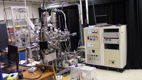
Laser-MBE and PLD system
Xiaoxing Xi, Temple University
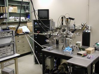
STM
Goran Karapetrov, Drexel University
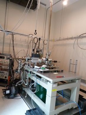
Scanning Tunnel Microscope
Maria Iavarone, Temple University
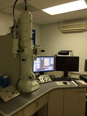
EOL-1400 TEM
Daniel Strongin, Temple University
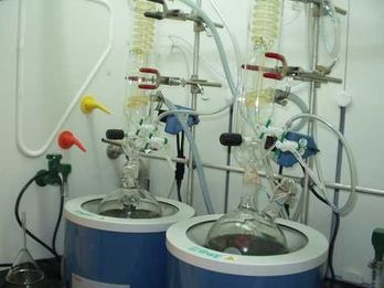
Sodium/Benzophenone Ketyl Scavangers
Michael Zdilla
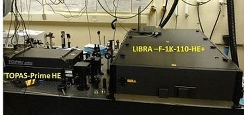
Femtosecond Amplifier System
Eric Borguet, Temple University